In the fast-evolving world of technology, where every nanometer counts, High-Precision 34-Layer Laser Blind Vias PCBs are carving a niche for themselves, especially in the realms of semiconductor testing devices and high-end consumer electronics. But what’s driving this demand?
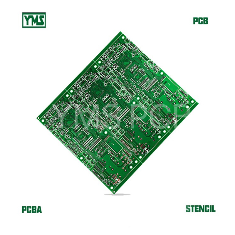
First, consider the advanced simulations and device miniaturization trends in the semiconductor industry. The precision offered by laser blind vias allows engineers to pack more functionality into smaller footprints, giving consumers the sleek devices they crave. Talk about few layers of magic!
Moreover, as the demand for high-end consumer electronics rises, manufacturers are seeking solutions that combine impressive performance with reliability. These 34-layer wonders not only meet but exceed the rigorous expectations of today’s savvy shoppers. The result? A surge in production lines buzzing with activity to cater to the new-age tech aficionados.
The dual application of these PCBs in both semiconductor testing equipment and consumer electronics presents an excellent opportunity for growth. The robust nature of these boards aids in precise testing, ensuring the components perform impeccably before hitting the market. And for the customers? Well, they're simply delighted with gadgets that work like a charm, every time! 🎉
In conclusion, the future of High-Precision 34-Layer Laser Blind Vias PCBs looks promising, not only for enhancing the performance of electronic devices but also for solidifying the market position of manufacturers willing to embrace this innovation. Isn’t it time you hopped on this express train to the future?


 284
|
284
|
 communication equipment
high-precision PCB
solutions
communication equipment
high-precision PCB
solutions
 164
|
Eco-Friendly PCB
Sustainable Development
Market Trends
164
|
Eco-Friendly PCB
Sustainable Development
Market Trends
 399
|
Antenna Technology
Power Module
Rigid-Flex PCB
Innovative Design
Complex Applications
399
|
Antenna Technology
Power Module
Rigid-Flex PCB
Innovative Design
Complex Applications
 344
|
Rigid-Flex PCBs
Industrial Automation
HDI Technology
344
|
Rigid-Flex PCBs
Industrial Automation
HDI Technology
 385
|
Aerospace
Flexible Circuit Boards
Reliability
385
|
Aerospace
Flexible Circuit Boards
Reliability


