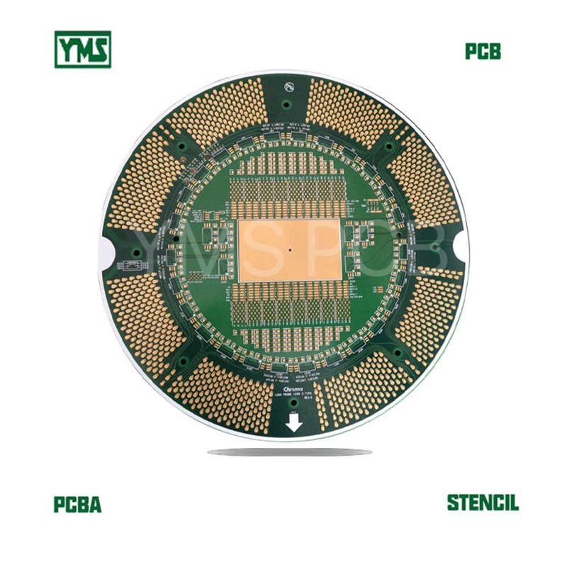
The High Precision 34-Layer Laser Blind Hole PCB produced by Mingzhenghong Electronics Co., Ltd. is engineered for superior performance in semiconductor testing and high-density electronic applications. Utilizing state-of-the-art back drilling and laser blind hole technology, this PCB guarantees exceptional signal integrity and reliability under rigorous operational conditions.
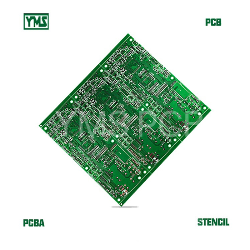
This PCB is meticulously crafted using FR-4 TG180 ITEQ (IT180A) material, achieving a board thickness of 5.0mm. It features a minimum hole diameter of 0.3mm, with minimum line width and spacing of 4mil (0.1mm) to support high-density circuit designs.
With an ENIG (Electroless Nickel Immersion Gold) surface finish, this product offers outstanding electrical conductivity and oxidation resistance. The outer copper thickness is 35um, with inner copper layers of both 18um and 35um, demonstrating superior durability and performance characteristics.

This PCB is specifically designed for a range of applications:
In conclusion, our High Precision 34-Layer Laser Blind Hole PCB stands at the forefront of technology, meeting the evolving needs of modern electronics. Please contact us for more information on how we can support your electronic design and production requirements.


 366
|
366
|
 Flexible FPC Boards
Industrial Automation
High-Frequency Signal Processing
Flexible FPC Boards
Industrial Automation
High-Frequency Signal Processing
 228
|
Flexible PCB
High-frequency applications
Rapid prototyping
PI polyimide
Flexible circuit boards
228
|
Flexible PCB
High-frequency applications
Rapid prototyping
PI polyimide
Flexible circuit boards
 290
|
Smart Manufacturing
High Conductivity
Thick Copper PCB
Power Management Systems
Smart Metering Devices
290
|
Smart Manufacturing
High Conductivity
Thick Copper PCB
Power Management Systems
Smart Metering Devices
 65
|
Multilayer PCB
High Conductivity PCB
Rigid PCB
FR-4 Circuit Boards
Thick Copper PCB
65
|
Multilayer PCB
High Conductivity PCB
Rigid PCB
FR-4 Circuit Boards
Thick Copper PCB
 270
|
High Precision PCB
PCBA
Soft and Hard Composite Plate
Green Manufacturing
Automotive Electronics
Medical Devices
270
|
High Precision PCB
PCBA
Soft and Hard Composite Plate
Green Manufacturing
Automotive Electronics
Medical Devices


